Description
PY32F003F1x TSSOP-20 Core Board – Bare PCB for DIY Soldering
Product Overview
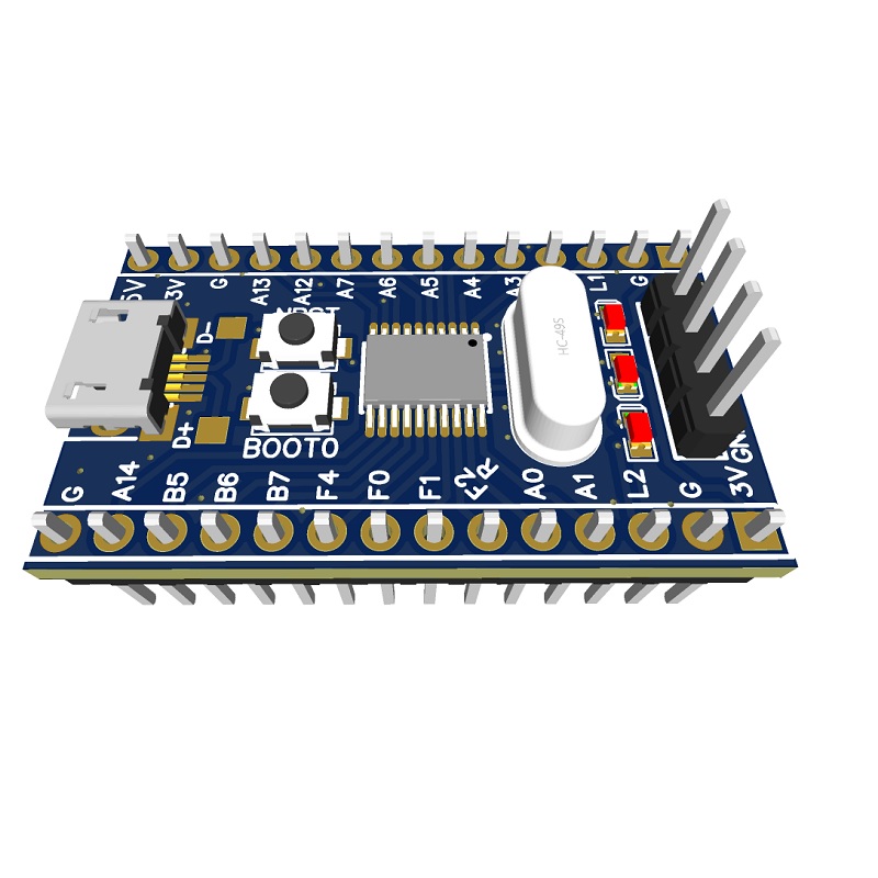
A compact PY32F003F1x development core board designed around the TSSOP-20 package, suitable for embedded systems, DIY electronics, prototyping, and low-cost ARM-based projects.
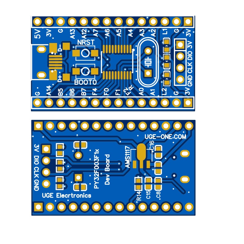
The board exposes all MCU pins through 2.54 mm headers and provides a dedicated 4-pin SWD connector for programming and debugging. It also provides convenient 3.3 V and 5 V power outputs, two user/test LEDs with jumper connections, and optional external crystal oscillator support.
This product is supplied as a bare PCB for DIY soldering.
Key Features
- Designed for PY32F003F1x MCU in TSSOP-20 package
- All MCU pins exposed through standard 2.54 mm headers
- Dedicated 4-pin SWD programming/debugging connector
- 3.3 V regulated output
- 5 V power output
- Three onboard LEDs:
- Power indicator
- L1 test LED
- L2 test LED
- L1 and L2 are accessible through header pins for flexible GPIO testing
- MCU can operate using its internal RC oscillator
- Optional external crystal/oscillator support
- Supports 16 MHz, 24 MHz, or 32 MHz external oscillator
- NRST/PF2 filtering capacitor can be omitted when the pin is required as a high-speed GPIO or alternate-function pin
- Compact core-board design for embedded and hobby projects
Technical Specifications
| Specification |
Details |
| MCU |
PY32F003F1x |
| Package |
TSSOP-20 |
| MCU Supply |
3.3 V |
| 5 V Support |
MCU supports 5 V according to the supplied design information |
| Regulated Output |
3.3 V |
| 5 V Output |
Available from board power input |
| Programming / Debugging |
SWD |
| SWD Connector |
4-pin |
| GPIO Access |
All MCU pins exposed |
| External Clock |
Optional |
| External Oscillator |
16 / 24 / 32 MHz |
| LEDs |
Power + L1 + L2 |
| Board Type |
Bare PCB / DIY Soldering |
Pin Access
All available PY32F003F1x pins are brought to the board headers, allowing the board to be used as a general-purpose development platform.
The header arrangement provides access to GPIOs including:
- PA0–PA7
- PB0–PB7
- PF0
- PF1
- PF2 / NRST
- PF4
Power connections include:
The exact alternate functions of each MCU pin depend on the PY32F003F1x device configuration and firmware.
SWD Programming & Debugging
A standard 4-pin SWD connector is provided for programming and debugging the MCU.
Typical connections are:
| SWD Pin |
Function |
| SWDIO |
SWD data |
| SWCLK |
SWD clock |
| 3.3V |
Target supply/reference |
| GND |
Ground |
The connector can be used with compatible SWD programmers/debuggers for firmware development and programming.
Power Supply
The board provides both 5 V and 3.3 V power connections.
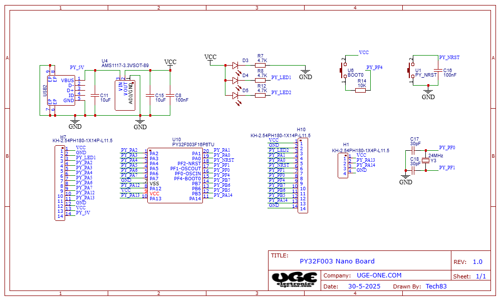
The onboard AMS1117-3.3 V regulator generates the regulated 3.3 V rail for the MCU and 3.3 V peripherals.
| Power Rail |
Description |
| 5 V |
Board input / available power rail |
| 3.3 V |
Regulated output from AMS1117-3.3 V |
| GND |
Common ground |
The PY32F003F1x operates from the 3.3 V rail in this board design.
Onboard LEDs
The board includes three LEDs.
| LED |
Function |
| Power LED |
Indicates that the board is powered |
| L1 |
External/test LED |
| L2 |
External/test LED |
L1 and L2 are not permanently assigned to specific MCU GPIOs. Their connections are brought to header pins so the user can connect them to the desired MCU pins using jumper wires.
This makes the LEDs useful for testing different GPIOs during development.
Clock Options
The board can operate using the MCU’s internal RC oscillator, so an external crystal/oscillator is not required for basic operation.
For applications requiring an external clock source, the board provides an oscillator connection supporting:
This allows the user to select the clock configuration according to the application requirements.
NRST / PF2 Configuration
The PF2 / NRST pin includes capacitor C16 (100 nF) for reset/noise filtering.
If the user wants to reuse PF2/NRST as a GPIO or another functional pin, do not solder C16.
C16 introduces a low-pass filtering effect on the pin and can reduce signals above approximately 10 kHz.
Therefore:
For normal reset operation: install C16.
For PF2 GPIO/high-frequency signal use: leave C16 unpopulated.
Typical Applications
- PY32 ARM development
- Low-cost embedded systems
- Sensor controllers
- Robotics projects
- DIY electronics
- GPIO experimentation
- Battery-powered embedded applications
- Industrial control prototypes
- Low-power applications
- Educational ARM microcontroller projects
- Custom PCB development
What’s Included
- 1 × PY32F003F1x TSSOP-20 Bare PCB
Bare PCB – DIY Soldering
This product is supplied as a bare PCB intended for DIY assembly.
Components are not soldered or included, unless specifically stated otherwise. The buyer can install the PY32F003F1x MCU, regulator, LEDs, connectors, oscillator components, capacitors, resistors, and other required components according to the schematic.
Notes
- MCU, connectors, LEDs, resistors, capacitors, regulator, and other components are not included with the bare PCB.
- The MCU is designed to operate from 3.3 V in this board configuration.
- An external crystal/oscillator is optional; the MCU can operate using its internal RC clock.
- If PF2/NRST is required as a GPIO or for signals above approximately 10 kHz, leave C16 unpopulated.
- Please refer to the PY32F003F1x datasheet for detailed electrical characteristics and alternate pin functions.









Reviews
There are no reviews yet.