Description
Overview
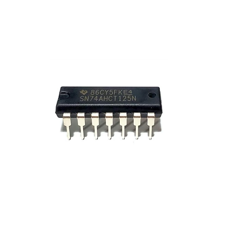
The SN74AHCT125N from Texas Instruments is a quadruple non-inverting bus buffer featuring four independent logic channels with 3-state outputs. Each channel can pass a digital signal from its input to its output or disconnect its output by using the individual Output Enable (OE) control.
The AHCT logic family features TTL-compatible inputs, making the device particularly useful for interfacing lower-voltage logic signals with 5 V logic systems. The device operates from a 4.5 V to 5.5 V supply and is available in a through-hole 14-pin PDIP package.
Key Features
- Quadruple non-inverting bus buffer
- 4 independent logic channels
- 3-state outputs
- Individual Output Enable (OE) for each channel
- TTL-compatible CMOS inputs
- 4.5–5.5 V supply operation
- Up to ±8 mA output drive
- Through-hole DIP-14 / PDIP-14 package
- Suitable for digital signal buffering and logic-level interfacing
- High-impedance output state when disabled
- Designed for bus-oriented applications
Technical Specifications
| Parameter |
Specification |
| Part Number |
SN74AHCT125N |
| Manufacturer |
Texas Instruments |
| Logic Family |
74AHCT |
| Function |
Quad Non-Inverting Buffer |
| Number of Channels |
4 |
| Bits per Channel |
1 |
| Output Type |
3-State |
| Input Type |
TTL-compatible CMOS |
| Supply Voltage |
4.5–5.5 V |
| Output Current |
±8 mA |
| Operating Temperature |
−40°C to +125°C |
| Package |
PDIP-14 |
| Mounting |
Through Hole |
| Package Width |
7.62 mm (0.300″) |
TI currently lists the SN74AHCT125N as an active device in a 14-pin PDIP package with a −40°C to +125°C operating-temperature range.
Logic Operation
Each channel operates as a non-inverting buffer:
| OE |
A |
Y |
| LOW |
LOW |
LOW |
| LOW |
HIGH |
HIGH |
| HIGH |
X |
High-Z |
When OE is LOW, the output follows the input. When OE is HIGH, the output is placed into a high-impedance (Hi-Z) state, allowing multiple devices to share a common bus.
Pin Configuration
| Pin |
Function |
| 1 |
1OE |
| 2 |
1A |
| 3 |
1Y |
| 4 |
2OE |
| 5 |
2A |
| 6 |
2Y |
| 7 |
GND |
| 8 |
VCC |
| 9 |
3Y |
| 10 |
3A |
| 11 |
3OE |
| 12 |
4Y |
| 13 |
4A |
| 14 |
4OE |
Power & Programming
- Supply voltage: 4.5–5.5 V
- Typical operation: 5 V
- No programming required.
- The device is controlled entirely through its digital inputs and Output Enable pins.
- A bypass capacitor should be placed close to the VCC and GND pins in practical PCB designs.
- Unused inputs should not be left floating; TI recommends tying unused inputs to VCC or GND.
Applications
- Digital bus buffering
- Logic signal buffering
- 3-state bus systems
- Microcontroller interfaces
- Logic-level interfacing
- Data bus isolation
- Memory and peripheral interfaces
- Signal distribution
- Digital control systems
- General-purpose 5 V logic circuits
What’s Included
- 1 × SN74AHCT125N Quad Non-Inverting Bus Buffer IC
- Package: DIP-14 / PDIP-14
- Through-hole
Notes
- The AHCT family uses TTL-compatible input thresholds, which makes it useful when interfacing logic signals to a 5 V system.
- Unlike a simple 74HC125, the 74AHCT125 should be powered from approximately 5 V within its specified operating range.
- The four channels are independently controlled through their respective OE inputs.
- When OE is HIGH, the corresponding output becomes high impedance rather than producing a logic HIGH or LOW.
- SN74AHCT125N is the TI PDIP-14 version; the same logic function is also available in other package variants.






Reviews
There are no reviews yet.