Description
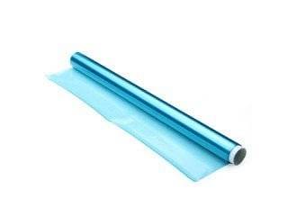
PCB Photosensitive Dry Film 15cmX20cm precut sheet pack of 10pcs
Feature:
Width: 15cm
Length: 20cM
1.5 mil thickness of dry film can be completely cover a hole of 0.25 inches
The dry film can be used in the most ordinary plating solution, no wrinkle, no discoloration
pack of 10pcs sale
Operating steps:
1, grinding CCL, this simple (PCB Photosensitive Dry Film sheet), using the finest polished clean water frosted paper on the line.
2, removing film, photographic film is sandwiched between two layers of film, the first side can make use of transparent tape tear torn, try a few on the line.
3, and then foil, copper clad laminates can look a little cleaner, pasted, try not to have bubbles.
4, good paste membrane used presses, not too hot, about 100 degrees from the fixing.
5, the printed circuit board film, suggestion is to use film, the fine could reach the highest degree of accuracy if you did not ask for the paper to print it with sulfuric acid trip.
6, the printed circuit on the photographic plate (Note: PCB Photosensitive Dry Film sheet is negative, so to highlight the print, which we usually use photographic plate opposite) with ordinary energy-saving lamps 10 or so, if there is exposure Machine 1 minutes on the line, the sun not tried, it should be 30 seconds -60 seconds, the exposure process Obviously, since the photosensitive film will change color when exposed to light, the light becomes dark blue. You will easily see your circuit diagram appeared on the board.
7, developing and tear the protective film on the front panel, into the developer (developer according 1:100,10 g Total 1L of water) to be used when developing a little harder stick cotton wipe board.
8, etching, this goes without saying (ferric chloride etchant environmental protection, hydrochloric acid + hydrogen peroxide, etc.) is recommended environmental etching shop, fast, clean, no odor.
9, after a good CCL etching, stripping, from film watered by 1:60 or 70, the board bubble like a few minutes,
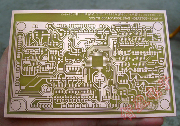
10, after the completion of the board, very pretty good, most dense line spacing is 0.1MM, width 0.1MM, 0.1MM lines do know though is very easy to do, but do 0.1 lines and 0.1 line spacing dry film can easily do it.
The following are the steps, and the detailed tutorial will be released later, which is quite easy to succeed.
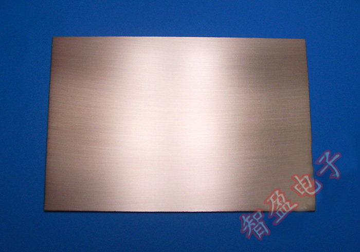
1. Polish the copper clad plate. This is simple, and it can be polished with the finest water sandpaper.
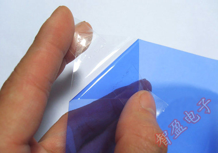
2, uncover the film, the photosensitive film is sandwiched between the two layers of film, first tear off one side can be torn by means of transparent adhesive tape, try a few more.
3, then film, a little copper plate can be cleaned, flat, try not to have bubbles.
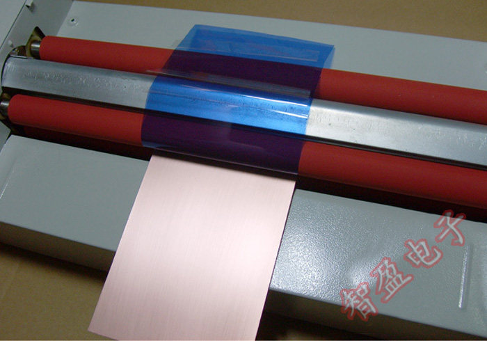
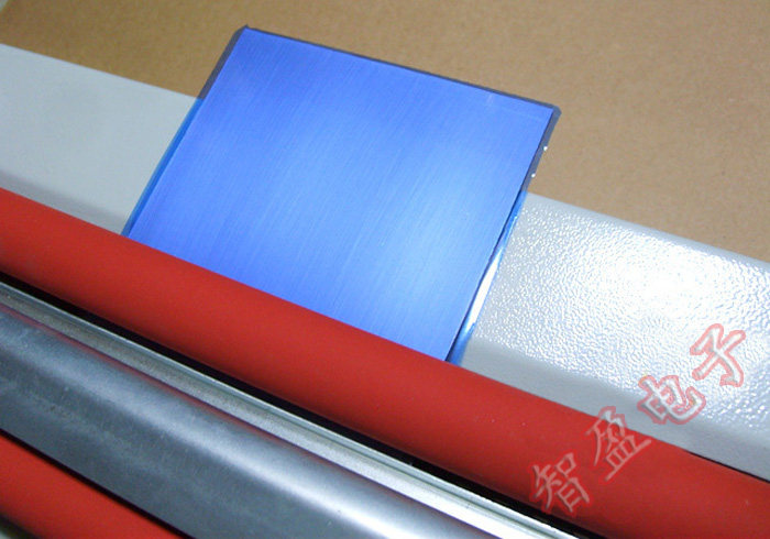
4, after the film is used, the plastic machine is used, not too hot, fixed at about 100 degrees.
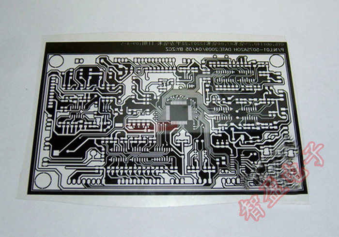
5, with inkjet film and laser film, you can achieve the highest fineness, if you do not require the use of sulfuric acid paper for printing accuracy. (The high precision is shown below )
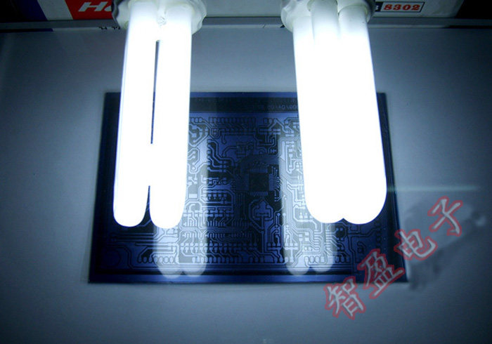
6, the printed circuit diagram is placed on the photosensitive plate, (dry film is negative, so to reverse printing, we provide 99SE and AD printing tutorial) energy-saving lamp exposure for about 8 minutes, exposure machine for 1 minute, the sun 30 seconds -Approximately 60 seconds, the exposure process is obvious, because the photosensitive film will change color when exposed, from light to dark blue. You will easily see your circuit diagram appear on the board.
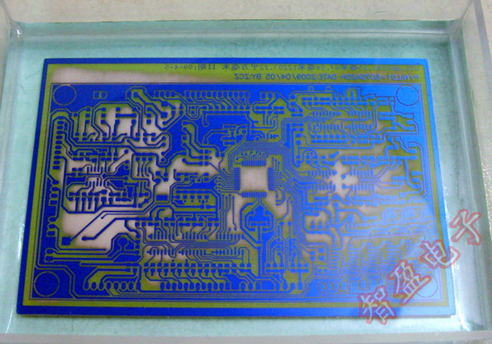
7. Development, tear off the protective film on the panel and put it into the developer (developer is 1:100, 10 g to 1 L of water). When developing, use a brush to wipe the board with a little force.

8, etching, environmental etchant water 1:4 fast, clean, no smell.
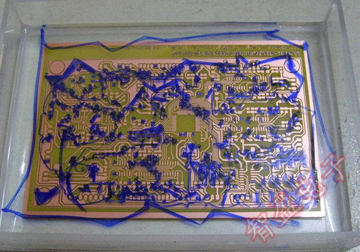
9. After the etched circuit board is stripped, remove the unnecessary film to expose the copper. The release agent is 1:50 water, soak it for a few minutes.
10, after the completion of the board, very good and very beautiful, the most dense line spacing is 0.1MM, line width 0.1MM, although it is easy to do 0.1MM line, but do 0.1 line and 0.1 line distance dry film It can also be easily made.






Ramadan Morsy (verified owner) –
Excellent product, recommended for student and amatures.